Communication systems rely on low-phase-noise signal sources such as tunable oscillators or phase-lock-loop (PLL) synthesizers for reliable voice communications and to ensure transmitted data integrity. Challenges still remain in achieving reasonable trade offs in low phase noise, low thermal drift, low power consumption, low cost, and potential for integration in integrated-circuit (IC) processes, however.1-38 With ever- increasing demands for high-speed data communications at rates in excess of 2 Gb/s,1-10 the phase-noise performance of the tunable signal source becomes critical in achieving acceptable system bit-error-rate (BER) performance.9 Fortunately, a design approach based on the use of selfinjection- locked compact coupled planar resonators (CCPRs) has been used to develop a line of high-performance, miniature RF/microwave signal sources that offer performance levels well suited to the demanding requirements of existing and emerging wireless communications systems.
Phase noise is a critical parameter for many electronic systems. For example, in short-distance radar systems, the capability to detect different targets as a function of time is dependent upon the phase-noise-performance of the system’s VCO module. Such systems require a high-performance VCO with low phase noise and high DC-to-RF conversion efficiency, and VCO designers are constantly asked to make trade offs between phase noise, power consumption, tuning range, interference immunity, size, and cost considerations.6-12
Constraints on high-quality factor (Q) resonator used in high-performance VCO circuits are particularly demanding, and a monolithic-microwave- integrated-circuit (MMIC) integrable solution has been the dream for decades.4 In general, a high Q resonator element is required to achieve low VCO phase-noise characteristics, but the realization of high Q resonator in planar form is difficult due to the higher loss characteristics of the resonator at high frequencies.
Dielectric resonators (DRs), for example, exhibit a high Q factor and have been used in high-spectral-purity signal sources at RF and microwave frequencies. Unfortunately, tunable oscillators based on DRs have been limited to narrow tuning ranges, are sensitive to vibration, high in cost, and not suited for current MMIC fabrication technologies.
An alternative, more cost-effective approach is to eliminate the DR and use a printed resonator, which is appropriate for use with current semiconductor manufacturing processes. Unfortunately, the phase-noise characteristics of VCOs based on printed resonators is inferior to VCOs using DRs since the Q of the DR is much higher than that of a printed resonator. 7-22 Planar resonators, such as ring, hairpin, spiral, and coupled resonators, can be easily implemented in a MMIC fabrication process, but with typically much larger size and lower Q than commercial DR-based oscillators. 2-10 The current work details research on a novel approach to improve the Q factor of a conventional printed resonator. The approach involves the use of a compact, modecoupling mechanism that is also well suited to MMIC processing.
Two available solutions are currently used for implementing highperformance VCOs. A DR-based VCO is usually the prime candidate for its high-Q performance at microwave frequencies. However, the DR requires precise machining for fabrication, and careful placement of the dielectric puck for optimal resonator coupling. This involves manual tuning of the DR for desired frequency operation. 7 The second approach involves fabricating an oscillator with MMIC techniques to produce a small, lowcost source, albeit with poor phase noise due to the low Q of printed resonators.1-10
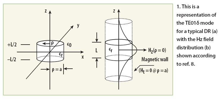
Although dielectric-resonator-oscillator (DRO) circuits have been widely used as high-performance signal sources, designers have sought to replace DRs with printed resonators in order to reduce size and cost.1-18 To review, a DR is a piece of dielectric material usually manufactured in a circular shape like disk or a cylinder with high relative dielectric constant (εr > 1) that acts as a resonant cavity by means of reflections at the dielectric/ air interface. Figure 1 shows the typical DR in a polar coordinate for giving brief insights about the possible resonant condition for a given parameters (L, a, εr). From ref. 8, it can be shown that by matching the tangential fields at the resonator interface (dielectric/air) at |z| = L / 2 , one can derive the following
where L = the length of the DR, a = the radius, εr = the relative permittivity, and c = the speed of light.
From Eq. 6, the transcendental equation yields two possible solutions for resonant wavelength, λ, but only one of these is valid in yielding a deterministic solution within the dielectric (λεr) and air (λεo).
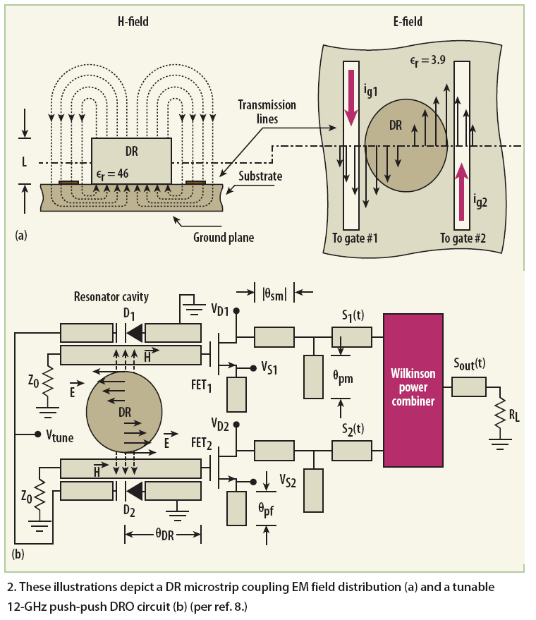
Figure 2 shows the typical high-performance DRO circuit using a DR in a push-push configuration. This design offers low phase noise but limited in tuning and poor subharmonic rejection.8 The exact placement of the DR disc between two parallel microstripline is critical, and slight variations can lead to higher harmonics and poor phase noise.
In addition to this, predicted DR resonant frequencies may differ from the measured results due to slight variations in temperature that cause problems during mass production and for integration of circuits. Such problems limit the usefulness of DRs. The frequency drift is not a straightforward function of temperature changes (due to different thermal expansion coefficients for cavity and dielectric pucks) and not easily corrected. The thermal sensitivity of a DRO can be reduced somewhat by the use of PLL circuitry and temperature control, although these are not integrable, cost-effective solutions.
Standard ICs are planar, so only those resonators having a planar structure are suitable for integration with such circuits.2-8 Unfortunately, integrable planar resonators are limited in Q and, therefore, in phase-noise performance. The poor phase-noise performance of a planar-resonatorbased VCO is due to the slow rate of change of phase and associated group delay characteristics of the resonator over the desire tuning range.
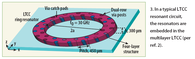
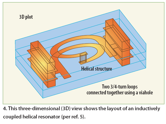
Recent publications explore the possibility to replace DR and techniques to improve the Q factor of the planar resonators for VCO applications, which have advantages for low cost, low phase hits, wide tuning range, and suited for on-chip realization.18-22 Resonators formed with lowtemperature- cofired-ceramic (LTCC) technology (Fig. 3) offer possible alternatives with high Q, and the technology can be adapted to MMIC processes, but it is difficult to integrate in a compact configuration.2 Printed helical resonators are also a possibility for good high-Q performance in small size at microwave frequencies. Figure 4 depicts the typical 3D layout of an inductively coupled helical resonator with two three-quarter-turn loops with via-hole connection.
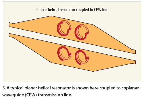
Edward5 proposed a novel, compact, high-Q multilayer integrable printed helical resonator that offers an optimum ratio of loaded quality factor to unloaded quality factor (QL/Q0 ) for minimum phase noise for a given VCO topology. Figure 5 shows an integrable planar helical resonator coupled to coplanar waveguide (CPW) for VCO applications.6 But such high-Q helical resonators are limited in tuning range for given phase-noise, size, and cost requirements.5,6
A recent publication11 described the design of an extended resonance oscillator (ERO) in which the resonator group delay is maximized for low phase noise. From ref. 6, the oscillator’s loaded Q factor, QL, is
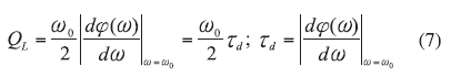
where
f(?) = the phase of the oscillator’s open loop transfer function at a steady state and
td = the group delay.
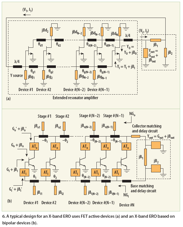
Figure 6 shows a typical ERO circuit using an N-way power divider and combiner where the condition for coherent power combining can be obtained by making phase difference between successive device output ports (Tdn) equal to the phase delay between the corresponding device input ports (Tgn).
From ref. 7, QL is proportional to the absolute value of the group delay; therefore, the main design objective for the ERO is to maximize group delay by incorporating (N >2) multiple devices. From ref. 11, the group delay td of the N-device ERO depicted in Fig. 3 can be described by
where
Ii = the input current,
I0 = the output current, and
V0N = the voltage at the output of the Nth device.
From ref. 11, the figure of merit (FOM), F, can be given by
where
td = the group delay and
L = the insertion loss.
The relative noise contribution of the N-device ERO circuit with respect to a two-device ERO can be given by11:
where
tDn = the group delay of the N-device ERO and
LN = the insertion loss of the N-device ERO.
From ref. 11, an eight-device ERO will yield about a 13-dB improvement in phase noise in comparison to a twodevice ERO, but there is a limitation in the number of devices for a given tuning range, noise factor, and power dissipation. The typical ERO circuit shown in Fig. 6 is limited to narrow/fixed frequency applications, sensitive to temperature variations, and requires larger real estate and power, therefore, not a promising alternative to DROs.
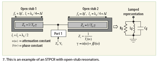
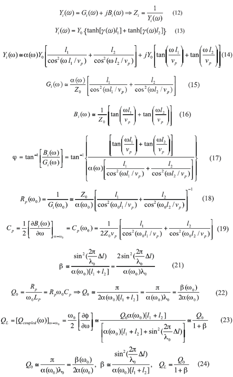
The new approach presented here simplifies the limitation of the ERO by incorporating a stub-based tuning mechanism to maximize the group delay for a given operating mode. The present work describes a novel topology that improves the Q factor in compact size, and also suited for MMIC process. Figures 7 and 8 show typical stub-tuned planar-coupled resonators (STPCRs). They use open and shorted stubs depending upon the injection strength for a given mode, operating frequency, and tuning range. Figure 7 shows open stubs of lengths l1 and l2 (l1,2 = ?0/4±?l) which form the self-coupling mechanism (without using a coupling capacitor). The two unequal planar open stubs exhibit resonant frequencies below and above f0, in which the lengths of the resonators are symmetrically offset by the amount ±Δl (Δl<λ0). This approach provides a selfcoupling mechanism without a lumped capacitor as a coupling element. The input admittance Yi(?) for this configuration is given by Eqs. 12-17.
where
Y0 = the characteristic admittance,
Z0 = the characteristic impedance,
vp = the phase velocity,
f = the phase shift,
?(?) = the propagation constant,
Gi(?) = input conductance, and
Bi(?) = input susceptance.
From ref. 15, Rp can be found by Eq. 18.
From refs. 14 and 16, Cp and Lp can be given by Eqs. 19 and 20 (Fig. 4 ):
Continue to page 2
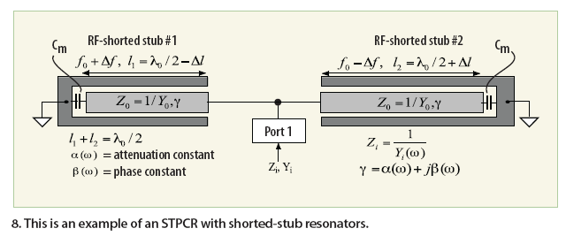
From refs. 18, 19, and 20, ß and Q factor can be given by Eqs. 21-23. From refs. 18-23, Rp, Cp, Lp, ß, and QL are dependent on the value of the offset length ±Δl of the open-stubtuned resonators. Similarly, the resonant characteristic of shorted stubs (l1,2=λ/2Δl) is given by Eq. 24.
The expression of phase noise, according to the discussion appearing on p. 332 in ref. 9, can be given by Eq. 25, where:
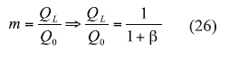
m = the ratio of the loaded and unloaded Q.
From eqs. 23 and 24, m can be given in terms of the coupling coefficient by using Eq. 26:
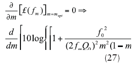
From refs. 25 and 27, the minimum phase noise can be found by differentiating Eq. 11 with respect to m, and equating to zero for minimum value of phase noise as Eqs. 27 and 28:
where
£(fm) = the ratio of the sideband power in a 1-Hz bandwidth at fm to the total power (in dB),
fm = the offset frequency,
f0 = the oscillator center frequency,
fc = the flicker corner frequency,
QL = the loaded Q,
Q0 = the unloaded Q,
F = the noise factor,
k = Boltzman’s constant,
T = temperature (in degrees K),
Po = average output power,
R = tuning diode equivalent noise resistance, and
Ko = voltage gain.
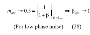
From ref. 28, for low-phase-noise applications, mopt and ßopt should be dynamically controlled and must lie in the vicinity of 0.5 and 1, respectively, for best phase noise.
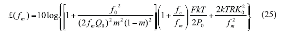
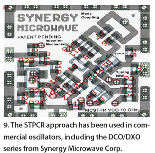
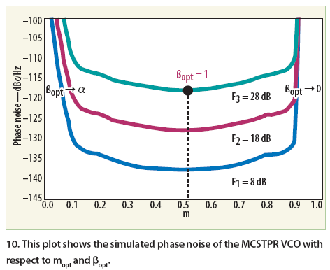
Figure 9 shows the typical layout of the DCO473542-5 (4.73 to 5.42 GHz), DXO810900-10 (8.1 to 10.9 GHz), and DXO10351090-5 (10.350 to 10.900 GHz) MCSTPR VCOs for the validation of the new approach by dynamically controlling mopt and ßopt for minimum noise figure. Figure 10 shows simulated phase noise for a 10-GHz MCSTPR VCO (Fig. 9) offset 1 MHz from the carrier with respect to mopt and ßopt .
From Eqs. 25 and 28, for different values of noise figure F (F3 > F2 > F1), the phase noise can be lowest for corresponding mopt = 0.5 and ßopt = 1, the plot is typically like a bathtub curve, shifted symmetrically about mopt .
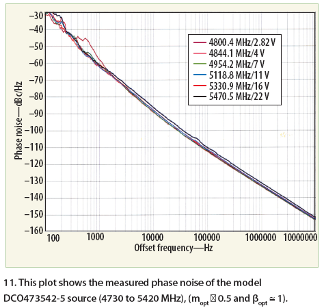
Figure 11 shows a measured phase noise plot of the discrete version of the MCSTPR VCO, typically –132 dBc/Hz offset 1 MHz from the carrier, within 3 dB of the simulated results.
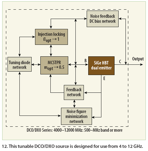
For validation of the novel MCSTPR approach, example tunable DCO/DXO VCOs using a SiGe heterojunction- bipolar-transistor (HBT) active device (a model BFP 740 from Infineon) were fabricated on Rogers substrate material with a dielectric constant of 3.38 and thickness of 30 mils (microstripline). Figure 12 shows a block diagram of the DCO/ DXO VCO series sources used for validating the the approach of achieving minimum phase noise performances over the operating band. The oscillators measure 0.35 x 0.35 x 0.16 in.
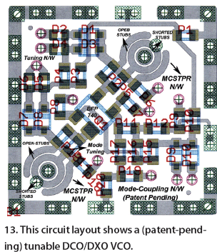
Figure 13 shows the layout of the tunable DXO10351090-5 VCO, where the MCSTPR sets up optimum standing waves (within the resonator) and the noise impedance transfer function over the tuning range (10.350 to 10.900 GHz) by controlling mopt (by optimizing injection-locking) and ßopt (by optimizing mode-tuning using open and shorted stubs).23-28
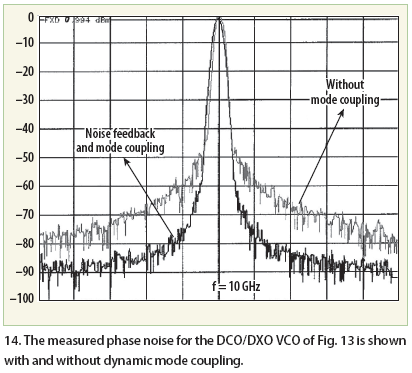
As depicted in Fig. 14, the dynamic mode-coupling mechanism exhibits 10 to 12 dB improvement in phase noise performance offset 10 kHz from 10-GHz carrier frequencies.
The measured RF power at 10 GHz is +1.2 dBm after compensating losses from the connectors and bias tee. The DXO circuit (Fig. 13) offers promising phase noise (better than –104 dBc/Hz offset 100 kHz) for broadband operation (10.350-10.900 GHz). Figures 15-31, on the online version of this article on www.mwrf.com, show measured performance for VCOs based on stub-tuned planar resonators, including the DCO473542-5 (4730-5420 MHz), DXO810900-10 (8100 -10900 MHz), and DXO10351090-5 (10350-10900 MHz).
This new approach to designing tunable oscillators with planar resonators yields compact VCOs with excellent phase-noise performance and in configurations that can be readily adapted to modern RF integrated circuit (RFIC) and MMIC semiconductor manufacturing processes.