Communication systems rely on low-phase-noise signal sources such as tunable oscillators or phase-lock-loop (PLL) synthesizers, both for reliable voice communications and to ensure transmitted data integrity. Constraints on source cost, size, power efficiency, and other performance parameters are particularly demanding. As data requirements increase beyond 2 Gb/s, the phase noise of one possible tunable source solution, the voltage-controlled oscillator (VCO), becomes critical for achieving acceptable bit-error-rate (BeR) performance. Fortunately, a design approach based on the patented technology1- 16 is the basis for a line of high-performance, compact VCOs from Synergy Microwave Corp. that offers performance levels well suited to the demanding requirements of existing and emerging wireless communications systems.
VCOs are versatile, tunable sources. Their resonators can be formed in a variety of ways, among them printing coupled resonators. VCOs reported in the literature with coupler planar resonators measure just 0.3 x 0.3 in. but can match the phase-noise performance of more expensive oscillators with high-quality-factor (high-Q) resonators. The planar resonator approach also lends itself to semiconductor fabrication processes, producing high-performance VCOs in integrated-circuit (IC) form.
The new VCOs offer 2:1 tuning bandwidths within the total range of 500 MHz to 18 GHz. These bandwidths support a wide variety of portable and fixed communications applications. In addition, these new distributed coupled resonator oscillators can be delivered at standard and custom frequencies without the non-recurring-engineering (NRE) costs associated with expensive custom-resonator-based oscillators. The new VCOs can also be designed into compact housings with low phase noise and optimized bandwidths to challenge the performance of high-Q ceramic-resonator, dielectric-resonator (DR), yttrium-iron-garnet (YIG) resonator, and surface-acoustic-wave (SAW) resonator oscillators—as well as low-Q resonators based on lumped circuit elements and printed transmission lines—but at about one-third the size.
Because one of the more difficult VCO parameters to optimize is phase noise, the source design team at Synergy Microwave targeted phase noise and bandwidth as key design challenges for the new compact coupled planar resonator (CCPR) oscillators. The result is several series of oscillators in the DCO and DXO series in compact housings measuring just 0.3 x 0.3 in. that are usable from -40 to +85°C in commercial, industrial, and military applications. They are available with narrow (about 10% tuning), moderate (about 50% tuning), and wide bandwidth (100% or greater tuning) frequency ranges.
The VCO product lines will be expanded for applications where power consumption must be controlled and supply voltages are limited to 2.1, 3, 3.3, 5, 8, 10, and 12 V and supply current as low as 10 mA. The DCO/DXO series VCOs are ideal sources for miniaturized PLL frequency synthesizers, with an outstanding combination of bandwidth and phase-noise performance. In addition, they are inherently immune to shock and vibration due to their use of printed coupled resonators—especially when compared to sources based on crystal, ceramic, SAW, DR, and YIG resonators.
The DCO/DXO series VCOs are RoHs compliant and can be delivered in tape-and-reel format for automated assembly processes. The VCOs are currently available in discrete-component form, but the technology is well suited for the transition to IC form.
Modern wireless communications depend on systems that can handle data rates of 2 Gb/s or higher.1-36 The bit-error-rate (BER) performance levels of these systems relies on the phase noise of the tunable oscillator, such as a VCO. Ideally, the VCO should have low phase noise, low cost, wide tuning range, and high DC-to-RF conversion efficiency. Synergy Microwave Corp.’s DCO/DXO series VCOs incorporate slow-wave-resonator (SWR) and mode-coupling techniques for high DC-to-RF conversion efficiency and low phase noise in small packages. As the name implies, slow-wave propagation takes advantage of guided-wave media with a slow phase velocity to transmit electromagnetic (EM) waves. The medium is typically a guided waveguide transmission line designed for a specific operating frequency. The use of such structures supports miniature oscillators, as well as evanescent-mode coupling for obtaining Q-multiplier effects at the resonant condition, for achieving low phase noise. The geometrical configuration of SWR resonators is also suitable for IC realization.
Because the use of a slow-wave structure can essentially shorten the required length of a transmission line at a target frequency, these structures are ideal for circuit miniaturization in oscillators. The use of periodic shunt loading can be used to reduce the phase velocity of a transmission line, thus increasing the effective electric length of the line. In conventional transmission lines, the phase velocity, Vp, is controlled only by the dielectric material and can be expressed24 as Eq. 1:
Vp = f? = C0/(µrerefff)0.5 (1)
where C0 = the velocity of light in the medium,
µr = the effective relative permeability, and
ereff = the effective relative permittivity of the dielectric material.
From Eq. 1, increasing the effective relative permittivity of the dielectric material at a given operating frequency will decelerate propagating EM waves in a guided medium. The slow-wave effect can be realized by adding periodical shields that decelerate the propagating EM waves in a guided medium.32
Equation 1 can be described with an equivalent inductance, Leq, equivalent capacitance, Ceq, and propagation constant, ß, as
ß = O(LeqCeq)0.5 ? VP = 1/(LeqCeq)0.5 (2)
From Eq. 2, both distributed inductance (L) and capacitance (C) along the transmission line in the guided medium can be increased for the realization of slow-wave effects, owing to an increase of the propagation constant, ß. Consequently, the loss of the resonator can be reduced.26
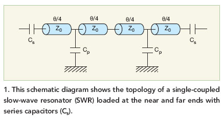
Figure 1 shows the typical simplified topology of a single-coupled slow-wave resonator. This consists of a slow-wave resonator loaded at its near and far ends with series capacitors, Cs. The resonator itself is made up of a transmission line of characteristic impedance Z0 and electrical length ?, periodically loaded by shunt capacitors Cp. The electrical length ? of the unloaded transmission line is defined at frequency f as Eq. 3:
? = ßd = [2pf(ereff)0.5/C]d ? ?|f = f0 = ?,0 (3)
where d = the physical length of the unloaded line and C = the velocity of light in free space.
At the center frequency, f0, the electrical length is ?,0. By using ABCD (cascade) matrices, the equivalent characteristic impedance, Zeq, of a coupled slow-wave resonator can be easily extracted. As shown in Fig. 1, the real estate of the SWR layout is quite large, and not suitable for applications where small size is critical.
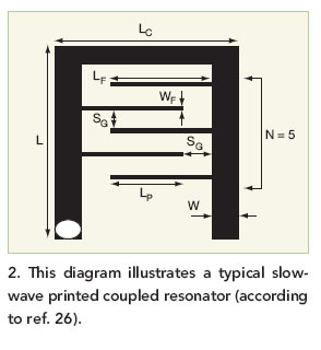
Figure 2 shows a typical layout for a printed SWR, capacitively coupled between two arms of the resonator leads to achieve the slow-wave effect. For unloaded transmission line, there is no dispersion in terms of phase velocity; however, for a periodically loaded line, phase velocity is frequency dependant.
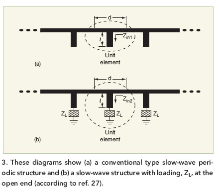
As illustrated in Fig. 3, the transmission line is periodically loaded with identical open-stub elements to realize a high-Q SWR structure.27 The input impedance, Zin2, for a lossless line can be given by Eq. 4:
Zin2 = Z0{[ZL + jZ0tan(ßl)]/[Z0 + jZLtan(ßl)]} Z0 = (L/C)0.5 (4) where L = the inductance per unit length of line, C = the capacitance per unit length of line, Z0 = the characteristic impedance of the open stub, and ß = the phase constant of the open stub.
If ZL = 8 or 0 with a very small value of tan (ßl), the input impedance Zin2 ? 8 or 0, respectively.27 Under these cases, the slow-wave periodic structure loaded by Zin2 in Fig. 1(b) provides passband (Zin2 ? 8) and stopband (Zin2? 0) characteristics.
As shown in Fig. 3, the resulting layout is somewhat large for tiny VCO applications. Figure 4 shows the modified SWR version, where the transmission line is loaded by a square ring resonator with a line-to-ring coupling structure. As depicted in Fig. 4(b), Zin3 is the input impedance looking into transmission line lb toward the ring resonator with line-to-ring coupling. The input impedance Zr1 looks into the line-to-ring coupling structure toward the ring resonator. The input impedance, Zin3, is given by Eq. 5:
Zin3 = Z0{[ZL + jZ0tan(ßlb)]/[Z0 + jZr1tan(ßlb)]} (5)
where
Zr1 = (Zr + Zg)Zp/(Zr + Zg + Zp), Zg = 1/ j?Cg?l, Zp = 1/j?Cp?l, j? = 2pf (6)
The parallel (fp) and series (fs) resonances of the slow-wave ring resonator as shown in Fig. 3 can be obtained by setting |Yin3| = 0 and |Zin3| = 0.
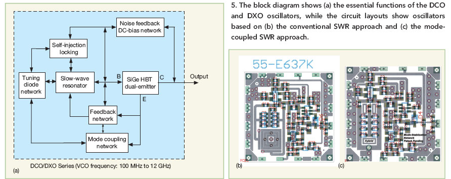
Figures 5(a), 5(b), and 5(c) show the block diagrams and layouts of DCO and DXO sources using a mode-coupled SWR. This validates the SWR approach, fabricating VCOs with a silicon-germanium (SiGe) heterojunction-bipolar-transistor (HBT) active device on a low-loss dielectric with dielectric constant of 3.38 and 22- mil-thick printed-circuit structure. The SWR structure was modeled by means of two-and-one-half-dimensional (2.5D) or three-dimensional (3D) EM simulator (Fig. 1) and incorporated into an optimized nonlinear oscillator circuit model.
The nonlinear circuit model is based on the oscillator transistor and its large-signal S-parameters. This partitioning of the oscillator into its modeled component parts works quite well, and the combination of the large-signal S-parameters and the nonlinear circuit model agrees closely with measured data from circuits already built. By using large-signal S-parameters, the transistor’s behavior can be analyzed under quasi-linear (low signal drive level) and nonlinear (large signal drive level) conditions, helping to improve circuit optimization with harmonic-balance simulation programs such as the ADS2010 software from Agilent Technologies and the Nexxim software from Ansys.
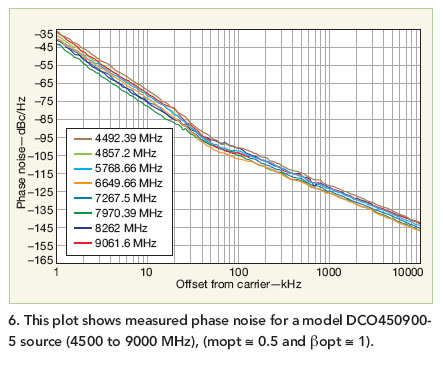
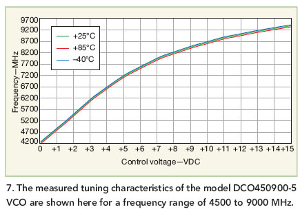
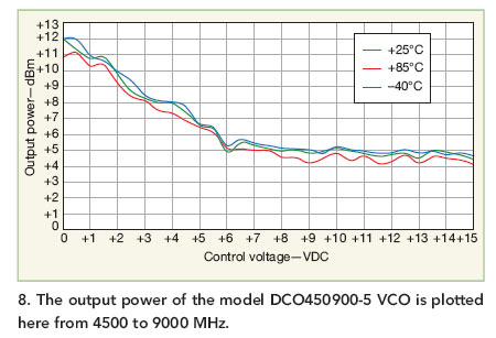
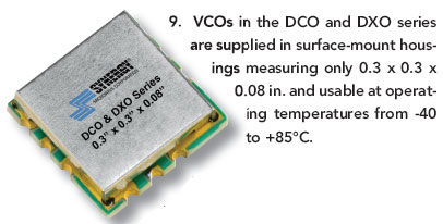
The SWR sets up optimum standing waves (within the resonator) and the noise impedance transfer function over the tuning range by controlling mopt (by optimizing injection locking) and ßopt (by optimizing mode tuning)(Fig. 5). The typical phase-noise performance, tuning characteristics, and output power characteristics for an octave-band, 4.5-to-9.0- GHz model DCO450900-5 can be seen in Figure 6, Figure 7, and Figure 8, respectively. The phase noise is -105 dBc/Hz offset 100 kHz from carriers of 4.5 to 9.0 GHz, for a tunable oscillator that fits within a compact surface-mount housing (Fig. 9) measuring just 0.3 x 0.3 x 0.08 in. Its performance levels are comparable to those of traditionally more-expensive high-Q resonator VCOs, with typical power consumption of only about 75 mW.
Additional models include the DCO50100-5, which tunes from 500 to 1000 MHz by means of tuning voltages of 0.5 to 15.0 V. It draws only 34 mA current at +5 VDC, but achieves phase noise of -100 dBc/Hz offset 10 kHz from the carrier. Model DCO5001000 tunes from 5 to 10 GHz and is available for +5- or +3-VDC supplies (only 20 mA current draw for each). It tunes by means of tuning voltages from 0.5 to 18.0 V and exhibits phase noise of -75 dBc/Hz offset 10 kHz for the +5-VDC supply and -73 dBc/Hz offset 10 kHz for the +3-VDC supply. At higher frequencies, model DXO11751220-5 tunes from 11.75 to 12.20 GHz by 0.5 to 15.0 V tuning voltages. It draws only 30 mA from a +5-VDC supply, while keeping phase noise to a low -80 dBc/Hz offset 10 kHz from any carrier in the frequency range.